
VIA CPU Overview
VIA CPU Overview.
VIA is, relatively speaking, a newcomer to the CPU market. After their acquisition of the Centaur division of IDT (bringing the Winchip) and of Cyrix they have put together a series of excellent CPUs. Via has admirably chosen not to join the chaos of performance desktop/server CPUs. This has kept them from having to compete with the likes of Intel and AMD. Rather they have concentrated on the quiet, cool, computing areas of small home boxes and laptops. These computers do not need to be able to play Doom 3 at 200fps or be able to rip DVDs day in and day out. They do however need to be very cool, and very quiet, fitting into small enclosures that do not have the capability of heating your entire house. VIA CPUs are designed for the digital media/security market. VIA can rightfully claim to have the 'coolest' CPUs available on the market.
VIA has released several cores and it can be hard to tell what makes them different.
VIA CPUs have been marked under the Cyrix name (which has now been dropped due to bad connotations with the massive heat generated by the late Cyrix MII) as well as '1GigaPro' and VIA's own name.
Thanks to VIA for donating several CPUs to the museum and making this page factually correct.
Individual Products:
Joshua
Samuel
Samuel 2
Ezra / Ezra-T
Nehemiah
Eden-N
Antaur-M
1GigaPro
Esther
CoreFusion
Bold CPUs are currently in production
Joshua
The Joshua (Cayenne NOT Jalapeno Core) was in the works at Cyrix as they were sold to VIA in 1999. The Joshua was a socket 370 CPU and was an evolution of the MII design. It was released in prototype form only.
| Core Process | .18u |
| L1 Cache | 64kB |
| L2 Cache | 256kB |
| Bus Frequency | 133MHz |
| Core Voltage | 2.2Volts |
| Thermal Dissipation | 20-25 Watts |
| Packages | CPGA (Socket 370) |
| Speeds | 333, 366, 400, 433, 450 |
| Pipeline | 7 stages |
| Core Name | Cayenne (aka Gobi) |
| Picture |
Samuel
The Samuel was VIA's rework of the old Winchip core. It was not a great performer due to the lack of L2 cache. The other major week point is that the FPU is clocked at HALF the CPU speed. The Samuel (and Samuel 2) retain the original 12 stage Winchip pipeline.
| Core Process | .18u Al |
| L1 Cache | 128kB |
| L2 Cache | 0kB |
| Bus Frequency | 100-133MHz |
| Core Voltage | 1.9 - 2.0 Volts |
| Thermal Dissipation | 11-20 Watts |
| Packages | CPGA (Socket 370) |
| Speeds | 500, 533, 550, 600, 650, 667, 700, 733, 750, 800 |
| Pipeline | 12 stages |
| Core Name | C5A |
| Picture |
Samuel 2
The Samuel 2 is fabbed by TSMC and is capable of using 3DNow and MMX instructions. It uses a very small 52mm square die which helps keep costs down. The Samuel 2 core is very simple but has excellent branch prediction (which is needed with such a small L2 cache). It has a much smaller die and power requirements then a comparative Intel (20 Watts) or AMD(25 Watts). I have run these chips without a heat sink or fan and they keep trucking just fine (this is not recommended). The Samuel 2 is really the first really successful CPU by VIA. It is more then capable of running any and all office app's as well as basic multimedia.
| Core Process | .15u Al |
| L1 Cache | 128kB |
| L2 Cache | 64kB |
| Bus Frequency | 100-133MHz |
| Core Voltage | 1.6-1.65 |
| Thermal Dissipation | 11-12 Watts |
| Packages | CPGA (Socket 370) |
| Speeds | 700, 733, 750, 800 |
| Pipeline | 12 stages |
| Core Name | C5B |
| Picture |
Ezra / Ezra-T
The Via Ezra was to be the next generation processor after the Via Samuel 2. The Ezra is produced on a .13 micron process. The bonus that Ezra has over the Samuel 2 is the ability to be clocked higher, and possibly to run cooler. There's really no major change between the Samuel 2 core and the Ezra aside from a smaller .13 micron process, lower voltage / power requirements and higher clock speed. The Ezra-T is merely a modification to be compatible with Tualitin sockets. The Ezra-T also transitioned to full copper interconnects (C5N core)
| Core Process | .13u Al/Cu -> Cu |
| L1 Cache | 128kB |
| L2 Cache | 64kB |
| Bus Frequency | 100-133MHz |
| Core Voltage | 1.35V |
| Thermal Dissipation | 15 Watts |
| Packages | CPGA (Socket 370) |
| Speeds | 800, 850, 866, 900, 933, 950 |
| Pipeline | 12 stages |
| Core Name | C5C: Ezra-T : C5M/C5N |
| Picture |
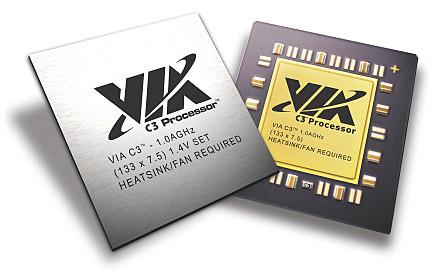
Nehemiah
.The VIA Nehemiah is still officially called the C3, but it uses the C5XL core developed by the WinChip team that Via acquired. Like previous Via C3 chips, it's aimed at the bottom of the market. The C5XL is the successor to the Ezra / C5C core and supports Intel's SSE extensions with 2 SSE units and a 16-stage pipeline. The FPU of the C5XL runs at full clock speed, unlike previous C3's which had 1/2 speed FPUs. With this the C3 can now perform almost as well as a Celeron or Duron but produces half the heat. The original Nehemiah core was the C5XL and that was the first to introduce an on-die RNG. The current core is the C5P and has two RNGs and an AES encryption engine. This is what is known as the "Padlock Data Encryption Engine"
It is of important note that only the C5P core has AES, this is core stepping 8 and VIA does not specify this when selling the CPU's. So many surplus or NOS EPIA motherboards have the older core. If you buy a new EPIA, you should have the AES engine, Use a CPUID program to be sure.
The Nehemiah began with the C5X core which had a core shrink resulting in the C5XL. The C5P added the second RNG.
All cores are .13u and use Cu interconnects. The Nehemiah also added 4 stages to the original C5 pipeline resulting a a 16 stage pipe.
| Core Process | .13u Copper |
| L1 Cache | 128kB |
| L2 Cache | 64kB |
| Bus Frequency | 100-133MHz |
| Core Voltage | 1.4-1.45 |
| Thermal Dissipation | 15-20 Watts |
| Packages | CPGA (Socket 370) EBGA |
| Speeds(GHz) | 1.0, 1.13, 1.2, 1.3, 1.4 |
| Pipeline | 16 stages |
| Core Name | C5X, shrunk C5XL, added AES - C5P |
| Picture |
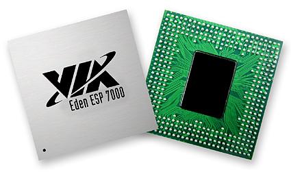
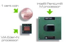
Eden-N & ESP
Eden CPUs are C3s that are fanless. What this means is that they dissipate 7 Watts or less of power. It uses a Nehemiah core on the .13u process in a VERY small (15mmx15mm) nano-BGA package. These CPUs run at barely 1Volt and dissipate a maximum of 7 Watts. This is unheard of in the range of 1 GHz CPUs. The Eden also offers very fast AES encryption (basically a quick random number generator).
THe Eden-ESP is a fanless C3 (7W or less) in a EBGA package whereas the Eden-N is a C3 in the Nano-BGA package. THey are for all accounts, the same CPU.
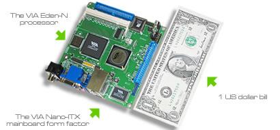
These are used on nano-ITX boards quite frequently. The CPU itself is smaller then a penny and about a quarter the size of the chipset. While the die is only slightly smaller then the Pentium M the package is 1/6th the size. This is CSP (Chip Scale Packaging) and is the future of CPUs. An entire motherboard for it is only 25 square inches. The remarkable point is power. The Eden can perform quite well for digital media application and only produces 7 Watts of heat at 1GHz. It is designed to run with no fan. It can be designed using a fanless powersupply as well. Thus a fanless, noiseless, thin PC with all of the customary x86 functionality.
The Eden-N is now used in Dual processor systems as well (how is that for slick)
The EPIA-DP supports DDR400, Gigabit Ethernet, and much more.
| Core Process | .13u Copper |
| L1 Cache | 128kB |
| L2 Cache | 64kB |
| Bus Frequency | 100-133MHz |
| Core Voltage | 0.8-1.0V |
| Thermal Dissipation | 7 watts max @ 1GHz |
| Packages | Nano-BGA |
| Speeds(MHz) | 533, 800, 1000 |
| Pipeline | 16 stages |
| Core Name | C5X, shrunk C5XL C5P |
| Picture |
Antaur
The Antaur is designed as a mobile CPU. Like the Eden-N it offers the worlds fastest AES x86 encryption in hardware. In today's world of high security this is highly needed and beneficial. It is a C5P Nehemiah core. The Antaur-M has full support of SSE, 3D Now! and MMX instructions. Once powered up the CPU can adjust its voltage dynamically by using PowerSaver 3.0 which is comparable to Intel's Speedstep Technology. Antaur CPUs also feature the NX flag to help defeat buffer overun exploits.
| Core Process | .13u Copper |
| L1 Cache | 128kB |
| L2 Cache | 64kB |
| Bus Frequency | 133- 200MHz |
| Core Voltage | 800mV for ULV 1.2 - 1.4V for others |
| Thermal Dissipation | 7W for ULV 11-19 for others |
| Packages | EBGA (368 Balls) |
| Speeds(GHz) | 1.00, 1.13, 1.2, 1.3, 1.33, 1.4 |
| Pipeline | 16 stages |
| Core Name | C5P |
| Picture |
1GigaPro
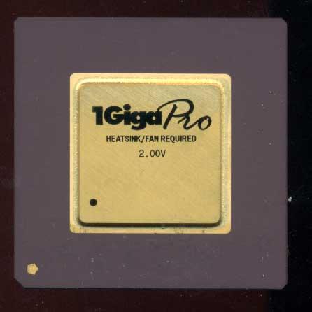
The 1GigaPro CPUs are VIA C3s that have been remarked by one of VIA's customers for use in very small boards (along the lines of the Mini-ITX form factor). The 1GigaPros will become rather collectible as they are not very common in comparison to other VIA chips.
Esther
VIA C7
The Esther using the C5J core is fabbed at an IBM fab (East Fishkill, N.Y.) rather then a TSMC fab like previous VIA chips. It features SOI and is made on a .09u process. This will allow a 1GHz chip to operate at about 3.5Watts. (24Watts at 2GHz)
The C5J alsos features RSA encryption, Secure Hashing and support for execution protection to help fight e-mail worms and viruses. The NX feature, according to Via, "marks memory with an attribute that code should not be executed from that memory," assisting the battle against malicious code. NX protection which will be supported with Windows XP SP2, was developed by AMD
The C7-M is the mobile version and has some impressive features.:
* Technical name: VSC7-M
* Its marketed in the same class as Celeron-M. (NOT Pentium-M)
* Small die size (1/3 of a Pentium-M)
* Hardware encryption (New features over C3)
* MPEG2/4 hardware accelerated (Due to chipset)
* 1.5Ghz, 1.1V, Max TDP : 10.1W (It rarely achieves this)
* 600MHz, 0.908V. (no problems with DVD playback)
* About 85 VIA engineers took the task of developing C7. (a rather small team)
* Support SSE/SSE2/SSE3, and NX bit.
* 128K L1 and 128K L2 Cache (256k L2 for the desktop version)
* FSB speeds: 800MHz (1066Mhz is possible if needed)
* Current speed is at 1.5GHz (will reach 2.0Ghz soon)
* Volume production should start at the end of the month.
* Runs two PLLs (marketing name: Twin Turbo)
* One PLL for the high clock speed, one at the lower one. (this is part of how it switches so fast)
* Can switch to high to low power modes in a single clock cycle.
(Pentium-M takes about 15K cycles to do the same)
As well as that, the core includes a front side bus of up to 800MHz, a larger L2 cache, and SSE2/SSE3 multimedia instructions.
| Core Process | .09u SOI |
| L1 Cache | 128k |
| L2 Cache | 256k (128k Mobile) |
| Bus Frequency | 800Mhz (1066MHz possible) |
| Core Voltage | 0.9-1.1V |
| Thermal Dissipation | 3.5W |
| Packages | BGA |
| Speeds(GHz) | 2.0 |
| Pipeline | ?? |
| Core Name | C5I/J |
CoreFusion
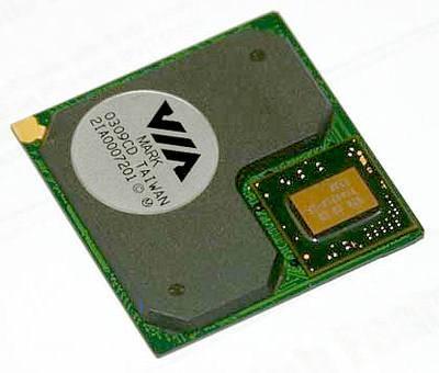
The VIA CoreFusion products are CPU's integrated with a chipset, similar to the cancelled Intel Timna CPU. VIA bega developing such CPU's in 2000 with the Matthew. The Matthew was canceled but its design led to the development of the Mark and Luke. The Mark can be considered Lukes little brother, it is the vaue plattform and lacks the Unichrome Graphics and other features that Luke has. Luke also runs up to 1GHz whereas Mark is limited to 533MHz.
The third generation is called "John"...I suspect this will use the C7 chip with newer CX700M or CN750 chipset. (This will support hardware accelerated WMV9, H.264, PCI-Express, DDRII 400/533 memory).
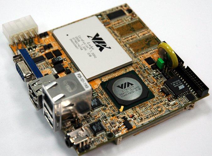
Note the massive heatsink, apparently it gets rather hot, but that is due to the chipset, and NOT the CPU.
| Matthew | Mark | Luke | John | |
| CPU | Samuel-II | Eden-N | Eden-N | C7-M? |
| Chipset | ?? | CLE266 | CN400 | CX700M or CN750 |
| Speed | ?? | 533MHz | 1GHz | |
| Voltage | ?? | 1V | 1V | |
| Release | 2000 | 2003 | 2005 | 2006 |
VIA CPU Feature Table
| Core ID | Core Name | Family, Model, Stepping | Speed (MHz) | Pipeline Stages | FPU Speed | Process |
| C5A | Samuel | 6.6.0 | 500-733 | 12 | 50% | .18u Al |
| C5B | Samuel 2 | 6.7.0-7 | 650-800 | 12 | 50% | .15u Al |
| C5C | Ezra | 6.7.8-f | 800-1000 | 12 | 50% | .15/.13 Hybrid Al |
| C5M | Ezra-T | 6.8.0 | 900-1200 | 12 | 50% | .15/.13 Hybrid Cu |
| C5N | Ezra-T | 6.8.0 | 900-1200 | 12 | 50% | .13u Cu |
| C5X | Nehemiah | 6.?.? | 1100-1300 | 16 | 100% | .13u Cu |
| C5XL | Nehemiah | 6.9.0-5 | 1000-1400 | 16 | 100% | .13u Cu |
| C5P | Nehemiah | 6.9.8 | 1000-1400 | 16 | 100% | .13u Cu |
| C5I/J | Esther | 1000-2000 | 100% | .09u Cu |
Note: Since the Eden is actually just a Nehemiah it is not listed in the table.
If you have any additional VIA CPU details and/or corrections please e-mail me.